0
登录后你可以
  • 下载海量资料
  • 学习在线课程
  • 观看技术视频
  • 写文章/发帖/加入社区
会员中心
创作中心
发布
  • 发文章

  • 发资料

  • 发帖

  • 提问

  • 发视频

创作活动
IPUH6N03LA G

IPUH6N03LA G

  • 厂商:

    EUPEC(英飞凌)

  • 封装:

    TO-251-3

  • 描述:

    MOSFET N-CH 25V 50A TO251-3

  • 详情介绍
  • 数据手册
  • 价格&库存
IPUH6N03LA G 数据手册
OptiMOS®2 Power-Transistor IPDH6N03LA G IPFH6N03LA G IPSH6N03LA G IPUH6N03LA G Product Summary Features • Ideal for high-frequency dc/dc converters • Qualified according to JEDEC1) for target application V DS 25 V R DS(on),max (SMD version) 6 mΩ ID 50 A • N-channel, logic level • Excellent gate charge x R DS(on) product (FOM) • Superior thermal resistance • 175 °C operating temperature • Pb-free lead plating; RoHS compliant Type IPDH6N03LA G IPFH6N03LA G IPSH6N03LA G IPUH6N03LA G Package PG-TO252-3-11 PG-TO252-3-23 PG-TO251-3-11 PG-TO251-3-1 Marking H6N03LA H6N03LA H6N03LA H6N03LA Maximum ratings, at T j=25 °C, unless otherwise specified Parameter Symbol Conditions Continuous drain current ID Value T C=25 °C2) 50 T C=100 °C 50 Pulsed drain current I D,pulse T C=25 °C3) 350 Avalanche energy, single pulse E AS I D=50 A, R GS=25 Ω 150 Reverse diode dv /dt dv /dt I D=50 A, V DS=20 V, di /dt =200 A/µs, T j,max=175 °C 6 Gate source voltage4) V GS Power dissipation P tot Operating and storage temperature T j, T stg T C=25 °C IEC climatic category; DIN IEC 68-1 Rev. 1.5 Unit A mJ kV/µs ±20 V 71 W -55 ... 175 °C 55/175/56 page 1 2008-04-14 Parameter IPDH6N03LA G IPFH6N03LA G IPSH6N03LA G IPUH6N03LA G Values Symbol Conditions Unit min. typ. max. - - 2.1 minimal footprint - - 75 6 cm2 cooling area5) - - 50 25 - - Thermal characteristics Thermal resistance, junction - case R thJC SMD version, device on PCB R thJA K/W Electrical characteristics, at T j=25 °C, unless otherwise specified Static characteristics Drain-source breakdown voltage V (BR)DSS V GS=0 V, I D=1 mA Gate threshold voltage V GS(th) V DS=V GS, I D=30 µA 1.2 1.6 2 Zero gate voltage drain current I DSS V DS=25 V, V GS=0 V, T j=25 °C - 0.1 1 V DS=25 V, V GS=0 V, T j=125 °C - 10 100 V µA Gate-source leakage current I GSS V GS=20 V, V DS=0 V - 10 100 nA Drain-source on-state resistance R DS(on) V GS=4.5 V, I D=30 A - 8.2 10.2 mΩ V GS=4.5 V, I D=30 A, IPD version - 8 10 V GS=10 V, I D=50 A - 5.2 6.2 V GS=10 V, I D=50 A, IPD version - 5 6 - 1.3 - Ω 35 69 - S Gate resistance RG Transconductance g fs |V DS|>2|I D|R DS(on)max, I D=50 A 1) J-STD20 and JESD22 2) Current is limited by bondwire; with an R thJC=2.1 K/W the chip is able to carry 80 A. 3) See figure 3 4) T j,max=150 °C and duty cycle D
IPUH6N03LA G
物料型号: - IPDH6N03LAG - IPFH6N03LAG - IPSH6N03LAG - IPUH6N03LAG

器件简介: OptiMOS®2 功率晶体管,适用于高频直流/直流转换器,符合JEDEC标准,N沟道,逻辑电平,具有出色的栅极电荷x R DS(on) 产品(FOM),卓越的热阻,175°C工作温度,无铅引脚镀层,符合RoHS标准。
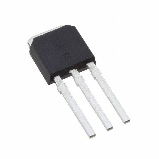
引脚分配: - drain pin 2 - gate pin 1 - source pin 3

参数特性: - 连续漏极电流:50A - 脉冲漏极电流:350A - 雪崩能量,单脉冲:150mJ - 反向二极管dv/dt:6kV/s - 栅源电压:±20V - 总功耗:71W - 工作和存储温度:-55...175°C

功能详解: - 热特性:结到外壳的热阻为2.1 K/W - 电气特性:包括静态特性和动态特性,如漏源击穿电压、栅阈值电压、栅源漏电流、漏源导通电阻、栅电阻、跨导等 - 反向二极管特性:包括连续正向电流、脉冲电流、正向电压和反向恢复电荷

应用信息: 适用于高频直流/直流转换器,并且符合JEDEC标准,说明这些器件适用于需要高效率和高频率的应用场景。

封装信息: - PG-TO252-3-11 - PG-TO252-3-23 - PG-TO251-3-11 - PG-TO251-3-1
IPUH6N03LA G 价格&库存

很抱歉,暂时无法提供与“IPUH6N03LA G”相匹配的价格&库存,您可以联系我们找货

免费人工找货